Blog number:-024
Hello Everybody.
I hope you all will be fine.
Today in this session we are going to discuss about Integrated Circuit which is 555 Timer IC.
555 Timer:-


So, that's all for this session. If you have any doubt related to the topic, please comment.
Hello Everybody.
I hope you all will be fine.
Today in this session we are going to discuss about Integrated Circuit which is 555 Timer IC.
555 Timer:-

The 555 timer IC is an integrated circuit (chip) used in a variety of timer, pulse generation, and oscillator applications. The 555 can be used to provide time delays, as an oscillator.
The 555 is the most popular integrated circuit ever manufactured. Introduced in 1972 by Signetics, the 555 is still in widespread use due to its low price, ease of use, and stability.
It has been falsely hypothesized that the 555 got its name from the three 5 kΩ resistors used within, but Hans Camenzind has stated that the part number was arbitrary. The "NE" and "SE" letters of the original parts numbers (NE555 and SE555) were temperature designations for analog chips from Signetics, where "NE" was commercial temperature range and "SE" was military temperature range.
Depending on the manufacturer, the standard 555 package includes 25 transistors, 2 diodes and 15 resistors on a silicon chip installed in an 8-pin mini dual-in-line package (DIP-8). Variants available include the 556 (a 14-pin DIP combining two 555s on one chip), and 558 / 559 (both a 16-pin DIP combining four slightly modified 555s).
The NE555 parts were commercial temperature range, 0 °C to +70 °C, and the SE555 part number designated the military temperature range, −55 °C to +125 °C.
The 555 timer chip is extremely robust and stable 8-pin device that can be operated either as a very accurate Monostable, Bistable or Astable Multivibrator to produce a variety of applications such as one-shot or delay timers, pulse generation, LED and lamp flashers, alarms and tone generation, logic clocks, etc, in fact any circuit that requires some form of time control as the list is endless.
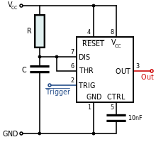
555 Timer Block Diagram
- • Pin 1. – Ground, The ground pin connects the 555 timer to the negative (0v) supply rail.
- • Pin 2. – Trigger, the OUT pin goes high and a timing interval starts when this input falls below 1⁄2 of CTRL voltage (which is typically 1⁄3 VCC, CTRL being 2⁄3VCC by default if CTRL is left open). More simply we can say that OUT will be high as long as the trigger is kept at low voltage. Output of the timer totally depends upon the amplitude of the external trigger voltage applied to this pin.
- • Pin 3. – Output, driven to GND or approximately 1.7 V below +Vcc. LEDs or motors can be connected directly to the output.
- • Pin 4. – Reset, This pin is used to “reset” the internal Flip-flop controlling the state of the output, pin 3. This is an active-low input and is generally connected to a logic “1” level when not used to prevent any unwanted resetting of the output.
- • Pin 5. – Control Voltage, This pin controls the timing of the 555 by overriding the 2/3Vcc level of the voltage divider network. By applying a voltage to this pin the width of the output signal can be varied independently of the RC timing network. When not used it is connected to ground via a 10nF capacitor to eliminate any noise.
- • Pin 6. – Threshold, the timing (OUT high) interval ends when the voltage at THR ("threshold") is greater than that at CTRL ( 2⁄3 VCC if CTRL is open). This pin connects directly to the RC timing circuit.
- • Pin 7. – Discharge, The discharge pin is connected directly to the Collector of an internal NPN transistor which is used to “discharge” the timing capacitor to ground when the output at pin 3 switches “LOW”.
- • Pin 8. – Supply +Vcc, the guaranteed voltage range of bipolar parts are typically 4.5 volt to 15 volts (some parts rated up to 16 volts or 18 volts).
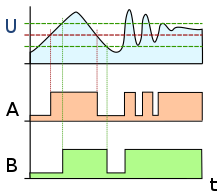
The 555 Timers have three 5kΩ resistors connected together internally producing a voltage divider network between the supply voltage at pin 8 and ground at pin 1. The voltage across this series resistive network holds the negative inverting input of comparator two at 2/3Vcc and the positive non-inverting input to comparator one at 1/3Vcc.
The two comparators produce an output voltage dependent upon the voltage difference at their inputs which is determined by the charging and discharging action of the externally connected RC network. The outputs from both comparators are connected to the two inputs of the flip-flop which in turn produces either a “HIGH” or “LOW” level output at Q based on the states of its inputs. The output from the flip-flop is used to control a high current output switching stage to drive the connected load producing either a “HIGH” or “LOW” voltage level at the output pin.
555 timer working
The 555 generally operates in 3 modes. A-stable, Mono-stable and Bi-stable modes.
Astable mode
This means there will be no stable level at the output. So the output will be swinging between high and low. This character of unstable output is used as clock or square wave output for many applications.Uses include LED and lamp flashers, pulse generation, logic clocks, tone generation, security alarms, pulse position modulation.
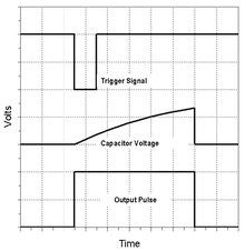
Mono-stable mode
This configuration consists of one stable and one unstable state. The stable state can be chosen either high or low by the user. If the stable output is set at high(1), the output of the timer is high(1). At the application of an interrupt, the timer output turns low(0). Since the low state is unstable it goes to high(1) automatically after the interrupt passes. Similar is the case for a low stable mono-stable mode. 555 functions as a "one-shot" pulse generator.
Bi-stable mode
In bi-stable mode, both the output states are stable. At each interrupt, the output changes from low(0) to high(1) and vice versa, and stays there. For example, if we have a high(1) output, it will go low(0) once it receives an interrupt and stay low(0) till the next interrupt changes the status.555 can operate as a flip-flop.
Specification:-
These specifications apply to the NE555
| Supply voltage (VCC) | 4.5 to 15 V |
| Supply current (VCC = +5 V) | 3 to 6 mA |
| Supply current (VCC = +15 V) | 10 to 15 mA |
| Output current (maximum) | 200 mA |
| Maximum Power dissipation | 600 mW |
| Power consumption (minimum operating) | 30 mW@5V, 225 mW@15V |
| Operating temperature | 0 to 75 °C |
Thank you.
No comments:
Post a Comment